Optical Sensor Project Overview
Several images may be right-clicked for a larger view. This page is best viewed at 1024x768 resolution.This sensor was developed to solve a key problem for a high volume sheet metal processing plant. Sheets of metal three feet square are coated with a protective lacquer, cut to size and welded together. The areas to be welded must be clear. When lacquer contaminates these areas, it will cause either a poor weld or costly damage to the welding electrodes. A key challenge was the inability to access the intended environment prior to development.
II Design Specifications
A) Function
- Design a sensor to detect contamination in a clear zone and detect wandering boundaries at the edges of the clear zone.
- Advise user of error detection and shut down machinery (Need external control outputs)
- Actual reject zone is narrower than margin sample (Must have precise data capture timing)
- Auto sheet sensing if possible (Must be able to sense everything from 0V to +5V)
- Custom circuit board with port for downloading new software
- Lights are on top of unit, and must be visible from either side of slitter
- Sheet speed handled should be at least 20 sheets/minute (Must have dynamic signal response)
- Self-calibrating with learn mode. Reject threshold half way between metal and lacquer voltages. Learn mode must "fuzz" sample lacquer boundary – minor width variations are acceptable (Must be able to store calibration constants)
- Unit pigtail cable should be at least 20 feet (Must retain signal integrity at a distance)
- Minimize the box size to reduce the leverage effect during sheet jams, causing misalignment.
- The most critical dimension is width, across the sheet or margin.
- All solid state design. MTBF should be far in excess of one year with few or no warranty claims. (Use an LED light source).
- Connectors on the outside of the unit to attach the power, output, reset line, remote learn button and for software downloads should be used.
- Environment may include dirty and poorly regulated power and both conductive and inductive noise, variable ambient light conditions and mechanical vibration for the sensors.
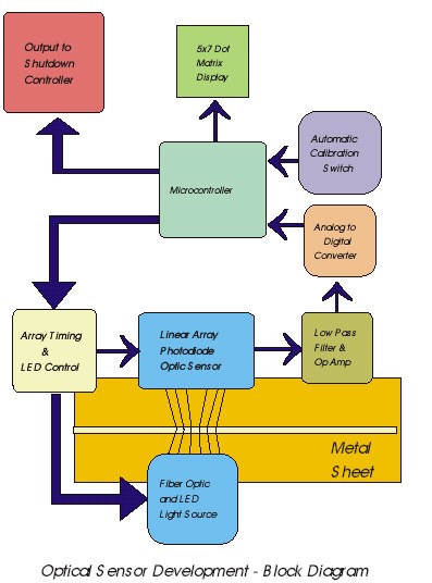
The block diagram shows the system and user inputs and outputs. It is drawn so as to emphasize the control signal generation, signal acquisition, and subsequent processing as a complete system loop. It may be referenced as each system function is discussed.
III Research
In order to verify that a system could be devised to detect the type of contamination involved in the process, the following research was completed:
- Internet research to isolate examples of suitable optical sensors.
- Contacting the appropriate vendors for part samples.
- Developing an evaluation platform capable of both qualifying the most suitable sensor and simultaneously establishing the viability of a monitoring concept.
- Acquiring metal samples with various lacquer coatings.
- Acquiring various colors of LED light sources to test light absorption characteristics at several wavelengths.
- Defining the sensitivity characteristics of the selected optical sensing component.
Once some initial light source, metal sample and optical sensor interactions were documented, the electronic signal processing circuitry was designed. This hardware-only approach was quickly defeated, as more complex signal signatures were observed which could not be accurately monitored without microprocessor and software management.
A PIC controller was selected for its numerous I/O ports and flash reprogrammability. It also featured an onboard Analog to Digital (A/D) converter and a Comparator. The A/D converter however requires far more time to acquire and convert a data sample than is available for real time processing. A hardware "flash A/D" was developed using a resistor ladder and a comparator tree. The onboard comparator and A/D converter are left unused as a result.
V Software DevelopmentInitially the center hump of the signal arising from the clear band was measured dynamically but when contamination was present the new servo would boost the signal back up to a passing level and no errors were detected. Assembly language was used to meet the demand for optimum timing efficiency by the real time data capture, analysis and response performance necessary.
As the code became more complex it was broken down into modules. This preserved the integrity of fully developed modules while more advanced system level refinements progressed.
A bit by bit sampling scheme was carried forward into a static measurement scheme. This method did work until it was discovered that the first 128 pixels of a given Linear Array do not have the same sensitivity to light as the second 128 pixels. The final development in measuring the center values was to average out the entire series of samples. A servo circuit accommodates a range of metal reflectivity, LED output intensities and Linear Array sensitivities. A key component in the loop is a digital potentiometer.
Changes in the design specifications called for the unit to have a user initiated auto calibration function. This prompted the development of software to utilize the EEPROM onboard the PIC. Registers were set aside for calibration constants and for the averaged value being used to represent the total center measurement of 32 pixels.
VI Debut PresentationThe unit was mounted to a moving slide rail above a representative metal sample. Sliding the unit over the sample simulated a fixed unit mounted over a moving sample. This module was exhibited at an International Exposition in Denver and was well received. Three months later, a revised PCB and housing assembly were mounted to the actual high volume sheet metal processing machinery. This was the first time the unit was ever exposed to the intended environment, and it worked flawlessly.
Table of Contents
Block Diagram Image 1
Light Source Selection on EVM Image 2
Color Reflectivity Testing on EVM Image 3 and Image 4
The Visible Spectrum, Color Addition and Absorption Images 5, 6, 7 and 8
Selecting a Narrow LED Source Image 9
How Colored Filters Cut Ambient Light Images 10, 11 and 12
Sensitivity Testing Linear Array Images 13 and 14
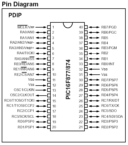
Selecting the PIC Microcontroller Image 15
Going with Assembly Language Modules, Timing is Limited and Critical
Onboard A/D Converter too Slow
Image 16
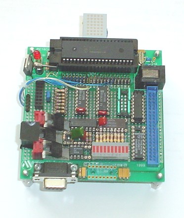
A Hand Wired Prototype Image 17
Dynamic Center Measurements Image 18
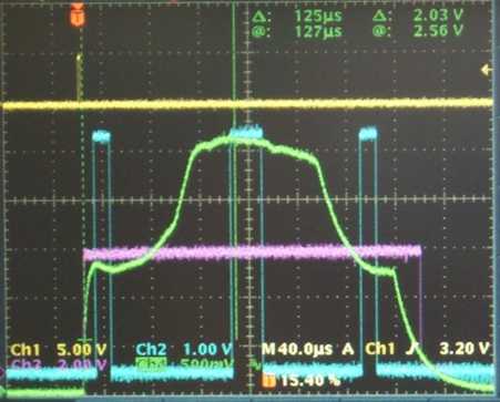
Magnified View of Signal Timing Image 19
Detecting Contamination Image 20
Low Pass Filter Image 21
Contact Information Contact

This is the first evaluation setup. It was effective in proving the concept that a distinction could be made between the clear metal and the lacquer coating. The left arrow shows the interface between the fiber optic cable, a metal sample and the Linear Array. The right arrow points to several different Light Emitting Diode (LED) colors being characterized to determine which would produce the most contrast and provide the illumination intensity required to generate a usable signal strength from the Linear Array.
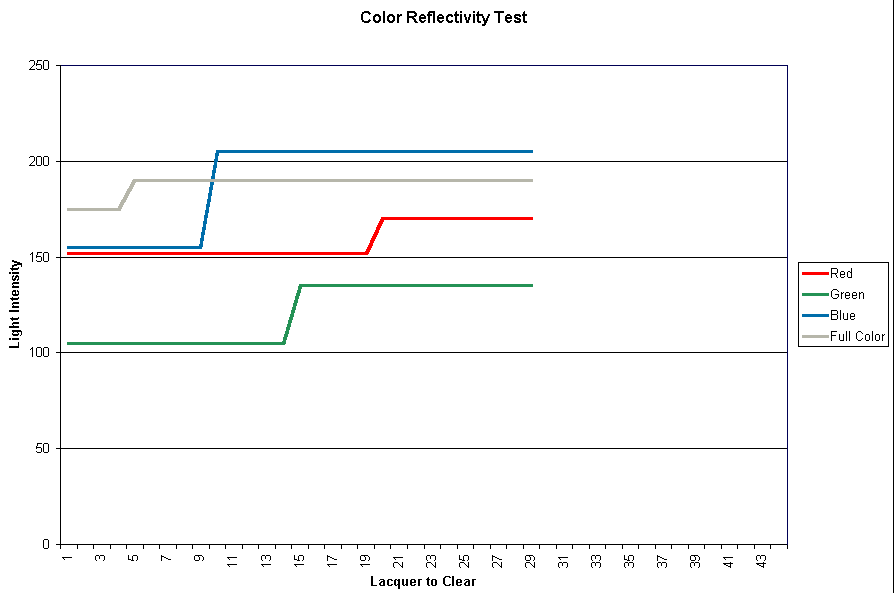
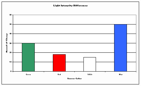
These columns indicate the differences in the amount of change between the different light source colors. The lacquer absorbs more blue light while the clear area reflects more of this color providing the most amount of change. This indicates how much more contrast can be produced between the clear metal and the lacquer coating on the metal using a blue light source.
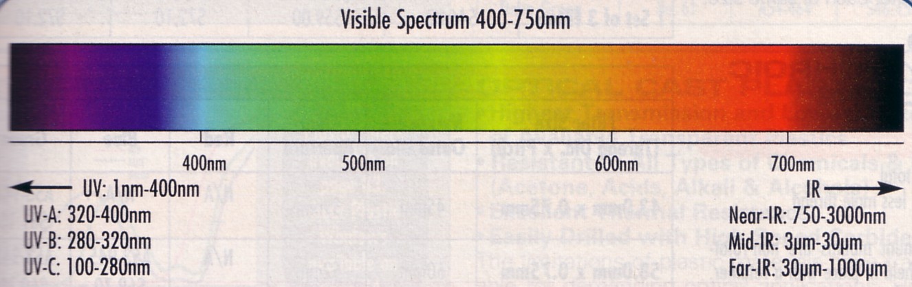
This is the full visible spectrum. It shows where the specific wavelengths of light referenced in this document are located relative to each other.

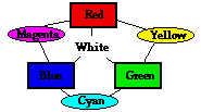
These circles show the effects of adding the primary colors of red, green and blue light together. The results produce magenta, yellow, cyan and white light.
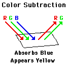
This shows the effects of absorption. Red, green and blue light strike the surface, but due to the absorption of blue, only red and green are reflected back from the surface. This is the same phenomenon, which produces the contrast range necessary for the optical sensor to work in detecting contamination on the metal sheets. Contamination will reduce the amount of light reflected back from what should be a clear area and alter the signal level expected to be present.

Based on the indications that blue light produced the most distinct contrast, a blue light source was selected. To meet the requirement that the unit have a Mean Time Between Failure(s) of one year, an LED was chosen as the light source. LEDs have a typical useful life expectancy of approximately 100,000 hours or nearly 11 years of continuous use. The graph above shows the narrow range of blue light produced by the high intensity blue LEDs shown above.
To enhance the response to blue light, a blue filter was selected to minimize the effects of any ambient light that may be scattered throughout the environment the sensor is operating in.
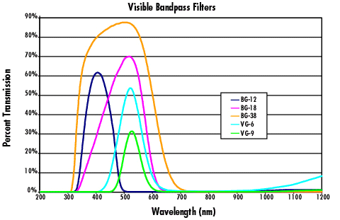
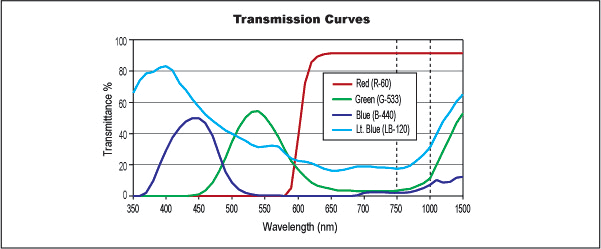
Different types of filters have varying degrees of effect upon the desired wavelength. Higher precision and narrower bandwidth are evident in the more expensive filter materials.
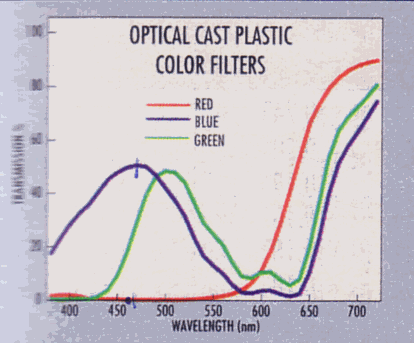
Lower precision and broader bandwidth are seen in lower quality plastic filters. These filters are useful due to their resistance to all types of chemicals and solvents. Exposure to these hazards prompted the use of this type of filter for the sensor.
This is the Linear Array Optical Sensor. It has two 128-photodiode segments a single 256 pixel row. Each segment or pixel is capable of sampling and storing a value of light intensity.
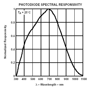
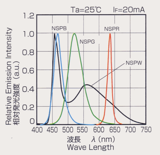
This is the spectral response curve indicating that the array has peak sensitivity to the red wavelength of 700 nanometers (700nM). The wavelength emitted by the blue LED is 470nM. The blue filter selected to protect the sensor from stray ambient light passes more light from the 470nM wavelength, while blocking other wavelengths of light present in the visible spectrum. This double protection eliminates the effects of stray ambient light, which could trigger a false response from the Linear Array due its stronger sensitivity to red light.
The processor chosen to control this sensor is the PIC16F877. It has many Input and Output ports (I/Os), internal timers and clocks, several permanent data storage locations (EEPROM), can be quickly erased and reprogrammed during development and in the field (flash memory) and several other features which led to this selection.
************************************************************************************
Assembly Language Code for the "Left Shoulder" Data Capture Sequence
************************************************************************************
Capture
Init_Left_Counters_Data_GPRsbcf STATUS, RP0 ; Bank 0
clrf Left_Count ; Clear Sample Counter
clrf Left_Avg ; Clear Sample GPR
movlw 0x40 ; Starting address for Left data samples
movwf FSR ; FSR Indirectly Addresses stored samples
Left_Sample_Pixels
clrf TMR1H ; Reset Timer1 High byte register
clrf TMR1L ; Reset Timer1 Low byte register to 0
btfss TMR1L, 3 ; Test for Left Shoulder Data start point
goto $-1 ; (8 counts + 1.0uS after SI) = Pixel 12
Trigger_Pulse1
bsf Pulse ; Set Port_A <0> as a trigger pulse
Left_Samples incf Left_Count, F ; Count number of samples
movf PORTD, W ; Capture sample values
movwf INDF ; Store data pattern in Left1
addwf Left_Avg, F ; Add up samples in a GPR
incf FSR, F ; Write next sample to next GPR (RAM) addr
Left_Sample_Count
btfss Left_Count, 0 ; Test Sample number
goto Left_Samples ; Capture only 1 Sample
bcf Pulse ; Clear Port_A <0> trigger pulse
The code above shows when a data sample capture begins by sending out a start marker (bsf Pulse) and an end marker (bcf Pulse). These markers can be seen in the photograph of the oscilloscope screen below.
The data sheet indicates that the A/D converter onboard the PIC would require approximately 20 microseconds (uS) to acquire the data. An additional 20uS more would be required to convert the data to a digital value. To compensate for this excessive time, a Flash A/D circuit using a resistor ladder and a series of comparators was devised. Using this scheme, the total time to Isolate, Capture and Store the data as a binary value is approximately 2uS. The Flash A/D approach is nearly 38uS faster (40uS - 2uS = 38uS). This is critical because an entire signal scan from the Linear Array is completed in 256uS (1uS per pixel). The data must be captured, stored, analyzed and produce a pass or fail result in real time.
This is a hand wired prototype built from a schematic representation of the circuit.
The image above is a photograph from an oscilloscope screen. It shows the primary control signals used in the Optical Sensor. The yellow trace is the main trigger pulse, called the SI Pulse. The cyan trace shows the Data Capture regions. The green trace is the signal from the Linear Array. The green center hump shows the highly reflective clear band bounded by two less reflective lacquer bands. The lacquer absorbing some of the blue light causes the lower reflectivity. The magenta trace shows the amount of LED Servo Drive Voltage being used to establish the proper LED intensity.
Continuous evaluation of the signal levels from these areas determines whether or not any lacquer has entered the clear band. When this occurs an immediate STOP signal is generated and the material is removed from the process.
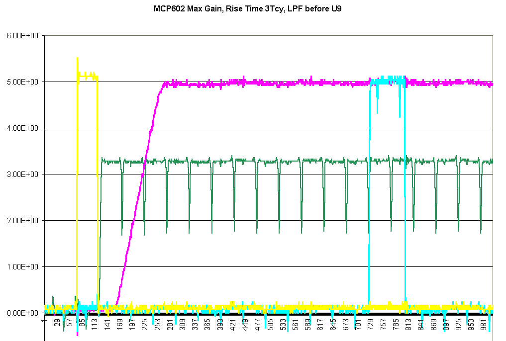
An extreme magnification shows the trigger pulse in yellow, the raw pixels from the Linear Array in green, the filtered and amplified signal in magenta and the first data sample, taken after pixel 12, in cyan. The sample is captured, measured and stored as a binary value in less than 2uS. Each pixel has a sampling time of 1uS. The MCP602 op amp is able to reach maximum gain in 3uS missing only the first 3 pixels after the raw signal is filtered and amplified. Since the first pixel sampled is number 12, this is not a problem. The op amp has a very high slew rate, ideal for operating at 5 volts. This allows all of the circuitry on the PCB to operate from a single supply.
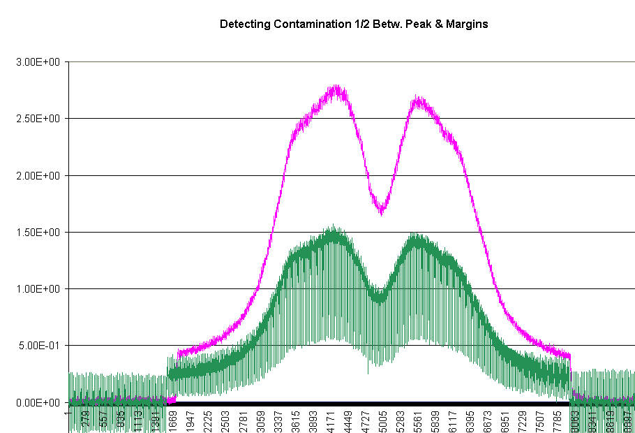
The magenta signal is the filtered and amplified signal from Linear Array Optical Sensor. The profile indicates the presence of contamination where the peak amplitude has a deep V-shaped notch. The green signal is the raw, unfiltered, unamplified signal from the Linear Array. The gain stage provides an amplification factor of approximately 1.8 times the original signal level.
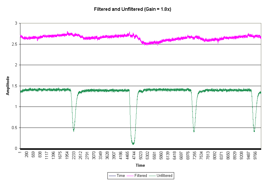
This chart shows the effectiveness of the Low Pass Filter (LPF). The original signal trace shown in green has a full 1-volt peak to peak (1V p-p) of noise excursions. The LPF reduces this to only 120 millivolts (120mV p-p), or 0.12 volts as seen in the magenta signal trace.